In one of my previous articles I wrote about how I set up an EEPROM programmer to write the code into the memory of my under construction computer. Now it’s time to make the very first test. We don’t need RAM memory yet, because at this stage we can just use only the internal registers of the CPU… and the non-volatile memory for the program, of course. For this test I purchased a Z80 PIO, a programmable parallel input/output interface which has two 8-bits ports that can be used to send/received data to/from an external device like a keyboard, an LCD display or similar. In this test I will simply light on a series of LEDs, just to see if I can send the classical “Hello, World!” message in an 8-bits way.
The Z80 PIO (Parallel Input/Output) has been made by Zilog specifically to work together with the Z80 CPU: in fact, it’s a member of the Z80 family, that includes other chips, like the CTC, the SIO and others. I discarded the MOS VIA that I initially thinked to use because it had been made to work with the 65xx family of CPUs from MOS and there were some issues to solve to have this chip working with my Z80, so I paid about 6/7 euros and bought a brand new Z80 PIO (yes! the Z80 family chips are still manufactured!).
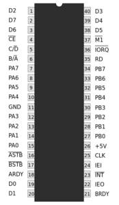
Here is the pinout of the PIO:
By choosing a chip from the Z80 family I got an important plus: I can connect directly the PIO to the Z80 CPU without additional chips. Below there are the most important wirings I have to make (a “/” before a name stands for an active low signal):
- D0..D7: the data lines – to be connected to the corresponding pins of the Z80
- /M1: in addition to its normal functions (it’s used as a sync pulse and to indicate when the CPU is fetching an instruction from the memory), the /M1 is used on the PIO in conjunction with /RD and /IORQ to reset the chip (by choosing the DIP40 format, Zilog had to sacrifice some lines, reset was one of these)
- /IORQ: used to inform the PIO that the CPU is accessing an input/ouput device
- /INT: used to send an interrupt reset to the CPU (but we won’t use it in this first tests)
- /RD: used to send a “read” signal to the PIO. The /WR pin is missing for the same reason of reset, so Zilog inserted a little circuit inside the PIO that creates the /WR starting with /RD (/WR is the inverse of /RD)
- CLK: to connect to the Z80 system clock
- B/A: this signal selects which port will be selected during a data transfer (port A or port B)
- C/D: this signal selects the type of data transfered between the CPU and the PIO, if a Control or Data byte.
- /CE: this is the “Chip Enable” line, to activate the PIO
There are a lot of other pins but, at the moment, we will forget about them because we won’t use them in this first test. I just remind you to connect a decoupling capacitor (0.1uF ceramic) between the +5V pin and ground, a 10K pull-up resistor on /IEI pin (this pin is used to set the PIO as the highest priority chip in the Z80 interrupt daisy chain structure).
By reading the datasheet of the PIO we can see that, when used as outputs, the PIO pins are not able to source big currents, even if the port B pins are able to drive Darlington transistors, so I opted to interface the port B with an ULN2803 Darlington transistor array, that can drive up to 500 mA, more than enought to light on 8 LEDs. To store our program I had 2 EEPROM chips, an AT28C256 from Atmel and an X28C256 from Hynix, both are 256 Kbit, or 32K x 8-bits. Obviously, you can choose a smaller size chip, too: keep in mind that, at the moment, the program is only some dozens of bytes in size! To connect the EEPROM to the CPU wire up the following lines:
- A0..A14 – to use the 32KB EEPROM we only need 15 address lines: the A15 pin of the Z80 CPU is left unconnected.
- D0..D7 – the data lines
- /WE – pull-up this line with a 10K resistor (it’s only used during programming of the EEPROM)
- /OE – connect it directly to the /RD pin of the CPU
- /CE – this is the chip select pin. Since there aren’t other memory chips yet, we can connect it directly to the /MREQ pin of the CPU so that the EEPROM will be selected when the CPU accesses the memory.
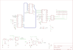
We’ve already seen the clock and reset circuit. So, connect the CLOCK pin of the CPU to the clock circuit and the /RESET pin to the reset circuit. Don’t forget the power lines (of course…) and the obiquitous decoupling capacitor. Lastly, connect the input lines of the ULN2803 to the PB0..PB7 pins of the PIO, connect the GND line (don’t connect the COM line), and wire up the LEDs: the anodes to 5V, the cathodes to the outputs of the Darlington array through some resistors (goods values range between 330 and 680 ohm). This is the final schematic:
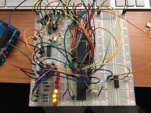
Now we can program the EEPROM by using our programmer. You’ll find the assembly source code on my GitHub repository soon, at the moment it’s not ready yet. At the end, power up the circuit and see the LEDs turning on and off in sequence, like a binary clock:
See you soon for the RAM tests…
Code & schematics can be found on this repository on GitHub.


