
Beyond the power lines, to work properly a CPU need some signals. The very basic ones are the reset and the clock signals. The former is used to… reset the CPU. This signal is generated both at the power up of the system and manually (i.e. by pressing a specific button). The reset is very important because sets the CPU in its starting status, clearing the internal registers and setting the external pins to high-Z state. The clock is as important as the reset: it is like a director, that gives the correct timings to all the instruments of the orchestra.
The first circuit that we will examine is the reset circuit. This is very easy to realize. It’s based on the widely used NE555 timer, one of the most long-lived integrated circuits. The NE555 has several working modes: in this particular task we will set it up to operate in monostrable mode, that is to say that the NE555 sets its ouput on a HIGH level for a certain time once a falling edge is detected on its input pin. The duration of the HIGH pulse can be set by combining a couple of external components, a resistor and a capacitor. The T time in seconds of the impuls is given by the following formula: T = 1.1 * R * C, where R is the resistor value in Ohms and C is the capacitance of the capacitor in Farad. This is needed because the reset signal must be active for at least 3 clock cycles before the reset operation is complete. But we will use the reset signal to reset the whole system so we will ensure that it will do its work properly by choosing a longer time. Since we don’t hurry to see our system up and running, I decided that we can wait for half a second. To achieve this, given the above formula, we can use a 47K resistor with a 10uF capacitor: in fact, T = 1.1 * 47K * 10uF = 1.1 * 47000 * 0.00001 = 0.517s. There is a little problem: the NE555 outputs an HIGH signal while the /RESET is an active LOW input: this means that it won’t function. But there is an easy solution: we just have to use a 7404 Hex Inverter that, like its name suggests, it simply inverts the input signal. By giving a LOW signal we get an HIGH one and vice-versa. So, when we will power up our system the NE555 will hold the reset line to LOW for half a second, giving the time at the whole circuit to have the voltage to a stable level. I also added a little switch to manually reset the system for our own needs.
Here is the schematic:

LM80C: reset circuit
R1 & C1 are used as a little anti-debounce filter for the switch. R3 is used as a pull-up resistor to give a stable HIGH value to the reset line when the NE555 is not working. When the 555 is triggered, i.e. after a power up or by pressing the switch, the timer will hold the output line HIGH for about 0.5s: since the output of the timer is connected to an input of the inverter, the RESET line will output a LOW signal until the timer will release its output, falling to LOW and, consequently, having the RESET line going to HIGH. It will be only in that moment that the CPU, and every other chip connected to the reset line, will start up.
The next step is to design a good clock circuit. The Z80 CPU needs a single phased clock signal, this means that, despite other microprocessor of its time that required two distinct clock signals (HIGH and LOW, separated on phase 1 and phase 2 line), it simply requires a square wave signal on a single line. The other important thing is the clock frequency, that directly impact on the speed of our CPU. The Z80 is a complex CPU and it has been designed to work with internal cycles called “machine cycles”: every instruction keeps at least 3 machine cycles (some 4 cycles), every cycle is composed of 4 clock cycles, so this is the reason why the Z80 has been always pointed as a slow CPU, if compared to 6502, for example: it needs more clock cycles. To achive good performances it has to work to higher frequencies than the rivals. In fact, the 6502 usually ran at about 1 MHz while the Z80 systems usually ran at 3.5/4 MHz. A common clock was 3.58 MHz because it is the clock of the NTSC colorburst. Several Z80 systems used the TMS9918 as the video processor chip: since this chip need an external quartz of 10.76 MHz to obtain the 3.58 MHz colorburst signal clock and since it could bring out that clock on an external pin, it was common and cheaper for the computer manufacturers use such clock as the system clock. MSX computers worked in such way. Instead, we will choose another frequency: since I thinked to connect the LM80C to a computer through the serial, and since the serial, to work properly, has some restrictions on the speed we can achive given a certain system clock, I opted for a 3.68 MHz clock, that is also not so far from the 3.58 MHz mentioned above. To obtain such frequency we will use a 7.37 MHz quartz: why will we do this? Why will we not simple choose a 3.68 MHz crystal? The reason is that we need to have a very stable square wave with a perfect duty cycle of 50% (the ratio of the HIGHs and LOWs periods of the wave). To achive this we will use a couple of ports of the hex inverter we had used for the reset reset. The 7404 is named “hex” inverter because it has 6 inverting ports. We use the inverter to stabilize the signal clock because the inverting port triggers only when the signal reaches a minimum voltage value. By using 2 inverting ports we are sure that the clock will be well stazilized and squared. We will also use a D-type flip flop to halve the 7.37 MHz clock so that we can obtain a good 3.68 MHz frequency. Here is the schematic:
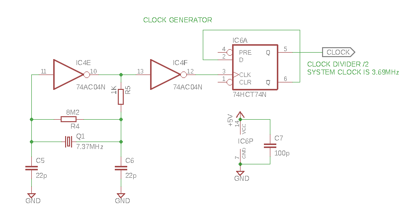
LM80C: clock circuit
C5 and C6 are needed to avoid the self-resonance of the crystal: these values are not absoluted, they depend on the crystal you chose, refer to its datasheet. The R4 is used to give the bias feedback to the inverting port. When the clock get out from the second inverting port is still at 7.37 MHz: by using the D-type flip flop, a common 7474 chip, we are going to halve such frequency to the 3.68 MHz required. I used my Arduino with the FreqCounter library to measure the clock:

Frequency check
Very stable, isn’t it?
So, we have done a good work, today. In the next article we will try to let our basic system do some little tasks. Stay tuned.
EDIT: I would spend some words about the CPU and the 74xx series chips. Zilog has made several versions of its CPU, they vary for the max clock they can work to and for the type of gates. The first models manufactured in the late 70s’ and the first years of the 80s’ were NMOS chips, later Zilog switched to CMOS manufacturing process. The latter can be recognized because they usually have a “C” inside the codename, i.e. “Z84C00”. Same for the peripheral chips: they both are non-CMOS and CMOS. A good rule is not to mix NMOS with CMOS parts because they have different capacitance on the pins. So if you buy a CMOS CPU, buy CMOS peripheral chips, too. And vice-versa: if you buy NMOS CPU, buy NMOS peripherals chips. Clock question: the Z80 was first built to work at a max. clock of 2.5MHz. The chip was simply marked as “Z80”. Later, Zilog manufactured other models that had different max. clock speeds: the “A” model can work up to 4MHz, the “B” model to 6MHz, the “H” to 8MHz. The old, original, CPUs have a letter after the name, i.e. Z80B. Newer models can work up to 25 MHz! They are usually marked with a codename, i.e. Z84C0006, where the 2 number at the most right indicate the max. clock speed: in this example, “06” stands for 6 MHz. For our purposes, choose a model that at least can work at 4 MHz, but 6 MHz is better. So a Z80B (if it’s from the past) or a Z84C0006 (if it’s manufactured today). Same for the peripheral chips: i.e., a PIO that can work at 6 MHz can be marked as “Z80B PIO” (old) or “Z84C2006” (new).
The 74xx series question. The 74xx family has been on the shelves for a long time, more than 40 years. During this period the manufacturing process has been changed several times. To work with our CPUs we need chips that are TTL-compliant, meaning that they can work with the TTL signals, 5V for HIGH and 0V for LOW. Moreover, they also differ for the max. current that can sink/source. In the past the “LS” series was used, but these chips are rare: fortunately, they can be replaced with “HCT” models. So, when I say that I’m using a 7404 I mean that I’m using a 74HCT04 chip. A so on. Keep this in mind when you look at my schematics, too. Many times, I didn’t find the proper components in the Eagle library so I used chips of the same type, with the same pinout, but of another family (i.e. AC instead of HCT) and I forgot to change the series’ code.
Code & schematics can be found on this repository on GitHub.