I was at a point where I couldn’t do more of these tests with what I’ve added to my little computer, so I decided to try to add an SRAM chip to use to store some data and the stack, that is necessary to be able to use the calls to sub-routines in my assembly programs. So I took an HM62256 chip from Hitachi and did some tests.
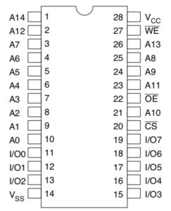
The HM62256 is a 256Kbit (32K x 8 bit) static RAM from Hitachi. Static means that it doesn’t need refreshing to retain the data stored inside it: by comparison, DRAM (Dynamic RAM) needs continuous refresh cycles otherwise they loose the data stored. The pinout is identical to that of the EEPROM so we can wire it easily, the only difference is the /WE pin: since this is a RAM, it’s writeable so we have to connect this pin to the /WR pin of the CPU.
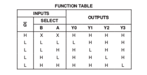
There is only a little problem. By connecting to the same address bus, the RAM will interfere with the ROM, and vice-versa, so we must develop a mechanism that lets the CPU select the correct chip where to read from/write to. This can be easily achieved using a 74139, a dual 2-to-4 address decoder/demultiplexer. This chip can select 1 out of 4 outputs from a 2-bits input address. It also has an enable pin so that we can enable it only when the CPU needs to perform a read/write operation to the memory. Here is it’s function table:
Our EEPROM and SRAM chips are both 32KB in size: since the Z80 CPU can directly address just 64KB of memory, we have to find a way so that the Z80 will see the chips one after another, going to fill up the whole address space. Which one has to be first? Easy answer: the ROM. Why? Because the Z80 is designed in a way that after a reset it will always starts at address $0000. Since the boot code needs to be stored in the non-volatile memory, this means that the ROM chip needs to occupy the first 32K of the address space and the RAM chip the second 32K. Looking at the chips we can also see that they only have 15 address pins while the CPU has 16 pins: in fact, 16 pins are needed to address 64KB (2^16=65,536 -> 64KB), while 15 pins can only address 32 KB (2^15=32,768 -> 32KB). So there’s an unused address pin, A15: we will use it to select between the ROM and RAM chips with our 74139 decoder. We’ll alse wire the /MREQ pin to the enable pin /G: doing this we will enable the decoder only for memory operations. By doing so, we have created an address decoder that selects the correct bank to read from/write to. To understand why this is so important let’s imagine this scenario: our CPU leaves the reset process and loads the $0000 into the PC (Program Counter) to fetch the instruction stored in such location. It would expected to access the ROM with some non-volatile code… but what if the CPU accessed the RAM at $0000 instead of the ROM? Unpredictable behaviors, since the RAM could have any random data at that address.
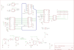
So, let’s start by modifying the previous circuit used for the Z80 PIO test:
As you can see, I’ve unwired the direct connection between the /IORQ pin of the CPU and the /CE pin of the PIO and opted to use the second side of the 74139 (keep in mind that it’s a “dual” decoder): at a first glance this could appear useless but we have to prepare our computer to manage other devices in the future so we can use the same mechanism adopted to decode the memory to address several peripherals, too. Let’s look a moment at the way the memory is decoded. Due to the fact that now we only have 2 chips that represent the 2 banks in which the memory has been splitted, we just need only 1 signal to select between them (the A15) so, since the decoder needs 2 inputs, I wired the other one to ground. By doing so, the decoder will select the ROM bank when A15 is LOW (address range from $0000 to $7FFF) while it will select the RAM bank when A15 is HIGH (address range from $8000 to $FFFF). This is easily verifiable by looking at the function table posted above. B is always LOW, so A (connected to A15) makes the selection: when it’s LOW, the decoder will enable the chip connected to the output marked as Y0 (the ROM bank) while when A will be HIGH it will enable the chip connected to Y1 (the RAM bank).
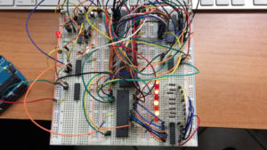
To finalize our project we load up a simple program that gets a pattern byte used to turn on the LEDs connected to our Z80 PIO and stores it into the first cell of the SRAM: its address inside the chip is $0000 but, thank to out decoding method of the addresses, it will be reachable at the logical address $8000. To be sure that the CPU addresses correctly the RAM, we change its value each time we read it. So what does our system do? The code, fetched by the EEPROM, reads a pattern byte from the SRAM, inverts its bits with a XOR operation, then sends it to the PIO that outputs it onto some LEDs. And so on. The correct SRAM access is proved by the LEDs that turn on/off alternatively, following the pattern of bits: this means that the CPU is able to store and retrieve such byte from the SRAM while it reads the instructions from the EEPROM. As you can see in the video below the described behaviour is exactly what we got, meaning that the memory decoding is functioning perfectly:
See you soon.
Code & schematics can be found on this repository on GitHub.


Sorry to leave a comment on such an old post but i am trying to get my head around the address decoding of the PIO.
In your schematic (and also in the schematic of the previous post) you connect the /CE pin of the PIO (through the decoder chip) to a combination of the /IORQ pin and the A4 address line. Why is the A4 line used here, since the /CE pin will already be low when only the /IORQ pin is low.
Correct me if i am wrong, but do you have now 8 IO-addresses (in combination with A0 and A1) to access the PIO where 4 would be sufficient?
Hello. You’re right. I could use only the IORQ line but since this is a path that I started to reach the goal of a complete system, I had to look forward, so I added the decoder in anticipation of the adding of other peripheral chips. If you continue to read in the next pages you’ll see that I will add a CTC, a SIO and other. A good start avoids you having to go back on your steps later, to re-project the decoder system. But sometimes planning isn’t enough: actually I’m using a 74138, a 3-to-8 decoder, since now I have 6 devices to address.
Thanks for your answer 🙂
I figured that out meanwhile and i think it’s a very neat mechanism to do this. I want to try myself designing something like this just for the sake of learning about the Z80 ‘stack’.