If we want to light on an LED connected to a pin of our Arduino we know that in order to do this we have to follow these steps:
1) set the pin as OUTPUT with the command pinMode;
2) “write” on that pin the value HIGH with the command digitalWrite.
This seems an easy job but if we check the code of the Arduino core we can see that it isn’t. The simplicity of the Arduino IDE permits to do this operation with just 2 instructions but in the background more operations are executed, because the Arduino core has to do several calculations to transform the pin number into the corresponding phisical pin and then it checks that this pin isn’t connected to a timer, in such a case it first has to deactivates the PWM signal if any. Only then the pin is set as requested.
If we don’t need a quick respond we can not take care about all of these steps, that are executed each time we call those instructions, but if we are looking for a fasted way to do these things there’s only a possibility: we have to directly manipulate the logic ports of the microcontroller.
A microcontroller is an electronics device so everything is done using digit informations. It has particular memory mapped registers that are used to set the phisical pins and that contain the status of every single I/O line of the microcontroller. A memory mapped register means that it is accessible by a particular memory address placed in an area of the SRAM memory that it isn’t used to store the program’s data. Each register represents a logic port: a logic port is combination of the bits connected to a group of phisical pins of the microcontroller. By reading/writing in these registers we can directly alter the pins status.
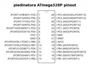
The logic ports of the Atmel AVR ATtiny & ATmega microcontrollers are 8-bits registers so every port contains the status of 8 pins of the chip.  On the right you can see the pinout of the ATmega328P, the microcontroller of the Arduino UNO: every pin is identified by a code like PD0, PC1, or PB2. For example, PD0 stays for the pin 0 of the logic port “D”. The ATmega328P has 23 I/O lines grouped in 3 logic ports named “B”, “C”, and “D”.
Every port is managed using 3 registers. Using the port “D” as example, we have:
- DDRD
this is a read/write register that contains the data direction of the connected pins. A (bit set to) 0 represents a pin set as INPUT while a (bit set to) 1 represents a pin set as OUTPUT; - PORTD
this read/write registers contains the status of the pins. The meaning of its values differ depending of the data direction:
– if the pin is set as INPUT, a 1 activates the internal PULL-UP resistor while a 0 deactivates it;
– if the pin is aset as OUTPUT, a 1 indicates an HIGH signal on the corresponding pin while a 0 indicates a LOW signal. - PIND
this is a read-only register and contains, when the pin is set as INPUT, the level of the signal that is entering the pin: bits are set to 1 per HIGH signales and set to 0 for LOW signals.
We can understand that if we want to set a pin as OUTPUT with an HIGH signal all that we have to do is set the direction of the pin with the DDRx register and then its status with the PORTx register. Don’t pay attention to the register addresses: the avr-gcc compiler will convert them into machine language instructions that will be able to read/write into the corresponding memory locations.
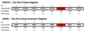
Let’s do a practical example. Let’s say we want to set the PD2 pin as OUTPUT with an HIGH signal. The picture below represents the registers that we’ll use with the affected bits marked in red: we’ll use the bit #2 (3rd position):
Into the DDRD register we will set to the bit DDR2 to “1” to set the pin PD2 as OUTPUT, while we will set the bit PORTD2 to “1” to have an HIGH signal on the pin.
The first way to do that is the following code:
DDRD = 0b00000100;

PORTD = 0b00000100;
It seems OK, isn’t it? No, it doesn’t! In fact, in this way we set ALL the bits of the 2 registers, altering every single I/O line of the PORT D, not only the one that we want to change. So, how can we do?
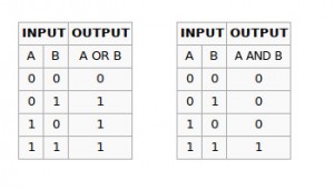
We can use the boolean algebra, in particular the OR and AND operators, or logical disjunction and logical conjunction, respectively. Let’s do a quick review of the truth tables of them:
Let’s analize the logic OR. It is sufficient that just one of the two values is true (1) to have a true result. Only when both values are false (0) the result of the OR is false too. Instead, the AND logic returns a true (1) value only when both of the two values are true, otherwhise the result will be false (0).
The OR is what we need to “light on” a single bit (set it to “1”): we only have to do an OR between the value of the bit and 1 to be sure that the result will be 1. To complete the job we need to use the binary shift operator too, <<. The syntax of this binary operator (it means that it works on the bits) is the following:
VALUE << SHIFT
It means: keep “VALUE” and shits it to the left by as many steps (bits) as the amount indicated by “SHIFT”. Here are some examples:
1<< 2 = 100

101<<1 = 1010

1111<<4 = 11110000
So, what did we have to do? We had to set as OUTPUT with an HIGH signal the pin PD2. The first thing to do is to set the pin as OUTPUT but without altering the rest of the bits of that port:
DDRD = DDRD OR DDD2
DDD2 is the bit in position #2 of the register so in C we’ll write a code like this:
DDRD |= (1<<2)
Let’s analize it starting by the part inside the round brackets: we tell the compiler to take the bit “1” and to shift it of 2 positions to the left. Then, we tell the compiler to take DDRD and to make a logic OR between its value with the result of the previous operations and finally to store the result in DDRD again.
DDRD = DDRD | 0b00000100
Using this method we will only alter the bit #2 leaving the other ones unchanged. Similarly, to get an HIGH signal on that pin we will use the following code:
PORTD |= (1<<2)
that is the same as
PORTD = PORTD | 0b00000100
Instead, to “light off” a bit we have to use the AND operator because it is sufficient to do a logic AND between 0 and the bit that we want to change to have as a result a false (0) value. The AND is more complicated to use than the OR because it can easily change all the bits due to the fact that it returns 1 only when both values are 1. We have to use another bit operator, NOT or ~. This operator inverts the value of a bit of the value of all the bits of a byte:
~1 = 0

~0b0001000 = 0b11110111

~0b11001100 = 0b00110011
So, let’s take the previous example and set a LOW signal on PD2 pin, that means we have to “light off” the bit #2 of the PORTD. To do that, we have to use together the AND and the NOT operators.
PORTD = PORTD AND ~PD2
that is the same as
PORTD &= ~(1<<2)
What does this code do? Let’s start resolving the operation between brackets, that gives 0b00000100 as a result. Now the operator ~ inverts the value of all the bits of the byte:
~0b00000100 = 0b11111011
The last operation is the logic AND between the value of the PORTD register and 0b11111011. Now, we know that an AND returns 1 only when both values are 1 and returns 0 when just one of the two values is 0, we can say that the only bit that will be affected is the bit we want to manipulate while the other ones will keep their original value. Let’s say the value of PORTD is 0b11001111, then the operation is:
PORTD &= ~(1<<2)
that is the same as:
PORTD = 0b11001111 & 0b11111011
Now PORTD gets the following value:
PORTD = 0b11001011
All the bit but the 3rd would keep their original value.


Un ottimo articolo propio im questo periodo mi sto interessando alla programmazione in c .
Tecno